Mssp Master Synchronous Serial Port

Pin direction. Most PIC microcontroller pins can be set as an input or and output and this can be done on the fly e.g. for a dallas 1 wire system a pin can be written.
- Blog Entry Interfacing the Microchip PIC18F Microcontroller Master Synchronous Serial Port MSSP to various I2C Devices December 11, 2011 by rwb, under.
- I2C are widely use for to communicate with external peripheral such as port expender, EEPROM, Real Time Clock etc. The Master Synchronous Serial Port MSSP.
- MSSP may refer to: Managed Security Service Provider, who provides security services for companies; Members of the Society of Specialist Paralegals.

5 Responses to Using Serial Peripheral Interface SPI with Microchip PIC18 Families Microcontroller.
The Enhanced Universal Synchronous Asynchronous Receiver Transmitter EUSART module is a serial I/O communication peripheral. It is also known as Serial Communications Interface SCI. It contains all clock generators, shift registers and data buffers necessary to perform an input or output serial data transfer independently of the device program execution. As its name states, apart from the usage of clock for synchronization, this module can also establish asynchronous connection, which makes it irreplaceable in some applications.
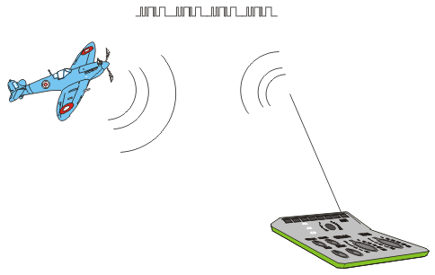
For example, in the event that it is difficult or impossible to provide special channels for clock and data transfer for example, radio remote control or infrared, the EUSART module presents itself as a convenient solution.
Fig. 6-1 Remote Control and Plane
The EUSART system integrated into the PIC16F887 microcontroller has the following features:
Full-duplex asynchronous transmit and receive;
Programmable 8- or 9-bit character length;
Address detection in 9-bit mode;
Input buffer overrun error detection; and
Half-duplex communication in synchronous mode master or slave.
The EUSART transmits and receives data using standard non-return-to-zero NRZ format. As seen in figure 6-2 below, this mode does not use clock signal, while the data format being transferred is very simple:
Fig. 6-2 EUSART Asynchronous Mode
Briefly, each data is transferred in the following way:
In idle state, data line has high logic level 1 ;
Each data transmission starts with START bit which is always a zero 0 ;
Each data is 8- or 9-bit wide LSB bit is first transferred ; and
Each data transmission ends with STOP bit which always has logic level which is always a one 1.
EUSART Asynchronous Transmitter
Fig. 6-3 EUSART Asynchronous Transmitter
In order to enable data transmission via EUSART module, it is necessary to configure it to operate as a transmitter. In other words, it is necessary to define the state of the following bits:
TXEN 1 - EUSART transmitter is enabled by setting this bit of the TXSTA register;
SYNC 0 - EUSART is configured to operate in asynchronous mode by clearing this bit of the TXSTA register; and
SPEN 1 - By setting this bit of the RCSTA register, EUSART is enabled and the TX/CK pin is automatically configured as output. If this bit is simultaneously used for some analog function, it must be disabled by clearing the corresponding bit of the ANSEL register.
The central part of the EUSART transmitter is the shift register TSR which is not directly accessible by the user. In order to start transmission, the module must be enabled by setting the TXEN bit of the TXSTA register. Data to be sent should be written to the TXREG register, which will cause the following sequence of events:
Byte will be immediately transferred to the shift register TSR;
TXREG register remains empty, which is indicated by setting flag bit TXIF of the PIR1 register. If the TXIE bit of the PIE1 register is set, an interrupt will be generated. Besides, the flag is set regardless of whether an interrupt is enabled or not. Also, it cannot be cleared by software, but by writing new data to the TXREG register;
Control electronics pushes data toward the TX pin in rhythm with internal clock: START bit 0 data STOP bit 1 ;
When the last bit leaves the TSR register, the TRMT bit of the TXSTA regis ter is automatically set; and
If the TXREG register has received a new character data in the meantime, the whole procedure is repeated immediately after the STOP bit of the previous character has been transmitted.
Sending 9-bit data is enabled by setting the TX9 bit of the TXSTA register. The TX9D bit of the TXSTA register is the ninth and Most Significant data bit. When transferring 9-bit data, the TX9D data bit must be written before writing the 8 least significant bits into the TXREG register. All nine bits of data will be transferred to the TSR shift register immediately after the TXREG write is complete.
Fig. 6-4 EUSART Asynchronous Receiver
Similar to the activation of EUSART transmitter, in order to enable the receiver it is necessary to define the following bits:
CREN 1 - EUSART receiver is enabled by setting this bit of the RCSTA register;
SYNC 0 - EUSART is configured to operate in asynchronous mode by clearing this bit stored in the TXSTA register; and
SPEN 1 - By setting this bit of the RCSTA register, EUSART is enabled and the RX/DT pin is automatically configured as input. If this bit is simultaneously used for some analog function, it must be disabled by clearing the corresponding bit of the ANSEL register.
When this first and necessary step is accomplished and START bit is detected, data is transferred to the shift register RSR through the RX pin. When the STOP bit has been received, the following occurs:
Data is automatically transferred to the RCREG register if empty ;
The flag bit RCIF is set and an interrupt, if enabled by the RCIE bit of the PIE1 register, occurs. Similar to transmitter, the flag bit is cleared by software only, i.e. by reading the RCREG register. Bear in mind that this is a two character FIFO memory first-in, first-out which allows reception of two characters simultaneously;
If the RCREG register is occupied contains two bytes and the shift register detects new STOP bit, the overflow bit OERR will be set. In this case, a new coming data is lost, and the OEER bit must be cleared by software. It is done by clearing and resetting the CREN bit.
Note: it is not possible to receive new data as far as the OERR bit is set;
If the STOP bit is zero 0, the FERR bit of the RCSTAregister detecting receive error will be set; and
To receive 9-bit data it is necessary to set the RX9 bit of the RCSTA register.
There are two types of errors which the microcontroller can automatically detect. The first one is called Framing error and occurs when the receiver does not detect the STOP bit at the expected time. Such error is indicated via the FERR bit of the RCSTA register. If this bit is set, it means that the last received data may be incorrect. It is important to know several things:
A Framing error does not generate an interrupt by itself;
If this bit is set, the last received data has an error;
A framing error bit set does not prevent reception of new data;
The FERR bit is cleared by reading received data, which means that check must be done before data reading; and
The FERR bit cannot be cleared by software. If needed, it can be cleared by clearing the SPEN bit of the RCSTA register. It will simultaneously cause reset of the whole EUSART system.
Another type of error is called Overrun Error. The receive FIFO can hold two characters. An overrun error will be generated if the third character is received. Simply, there is no space for another one byte and an error is unavoidable. When this happens the OERR bit of the RCSTA register is set. The consequences are the following:
Data already stored in the FIFO registers two bytes can be normally read;
No additional data will be received until the OERR bit is cleared; and
This bit is not directly accessed. To clear it, it is necessary to clear the CREN bit of the RCSTA register or to reset the whole EUSART system by clearing the SPEN bit of the RCSTA register.
In addition to receiving standard 8-bit data, the EUSART system supports 9-bit data reception. On the transmit side, the ninth bit is attached to the original byte just before the STOP bit. On the receive side, when the RX9 bit of the RCSTA register is set, the ninth data bit will be automatically written to the RX9D bit of the same register. When this byte is received, one should take care of how to read its bits- the RX9D data bit must be read before reading the 8 least significant bits of the RCREG register. Otherwise, the ninth data bit will be automatically cleared.
When the ADDEN bit of the RCSTAregister is set, the EUSART module is able to receive only 9-bit data, whereas all 8-bit data will be ignored. Although it seems like a restriction, such modes enable serial communication between several microcontrollers. The principle of operation is simple. The master device sends 9-bit data which represents the address of one microcontroller. All slave microcontrollers sharing the same transmission line, receive this data. Of course, each of them must have the ADDEN bit set because it enables address detection.
Upon receiving this data each slave checks if that address matches its own. Software, in which address match occurs, must disable address detection by clearing its ADDEN bit. The master device keeps on sending 8-bit data. All data passing through the transmission line will be received by recognized EUSART module only. Upon receiving the last byte, the slave device should set the ADDEN bit in order to enable new address detection.
CSRC - Clock Source Select bit - determines clock source. It is used only in synchronous mode.
1 - Master mode. Clock is generated internally from Baud Rate Generator; and
0 - Slave mode. Clock is generated from external source.
TX9 - 9-bit Transmit Enable bit
1 - 9-bit data transmission via EUSART system; and
0 - 8-bit data transmission via EUSART system.
1 - EUSART operates in synchronous mode; and
0 - EUSART operates in asynchronous mode.
SENDB - Send Break Character bit is only used in asynchronous mode and only in case it is required to observe LIN bus standard.
1 - Sending Break character is enabled; and
0 - Break character transmission is completed.
BRGH - High Baud Rate Select bit determines baud rate in asynchronous mode. It does not affect EUSART in synchronous mode.
1 - EUSART operates at high speed; and
0 - EUSART operates at low speed.
TRMT - Transmit Shift Register Status bit
1 - TSR register is empty; and
TX9D - Ninth bit of Transmit Data can be used as address or parity bit.
1 - Serial port enabled. RX/DT and TX/CK pins are automatically configured as input and output respectively; and
RX9 - 9-bit Receive Enable bit
1 - Receiving 9-bit data via EUSART system; and
0 - Receiving 8-bit data via EUSART system.
SREN - Single ReceiveEnable bit is used only in synchronous mode when the microcontroller operates as master.
1 - Single receive enabled; and
CREN - Continuous Receive Enable bit acts differently depending on EUSART mode.
1 - Enables continuous receive until the CREN bit is cleared; and
0 - Disables continuous receive.
ADDEN - Address Detect Enable bit is only used in address detect mode.
1 - Enables address detection on 9-bit data receive; and
0 - Disables address detection. The ninth bit can be used as parity bit.
1 - On receive, Framing Error is detected; and
1 - On receive, Overrun Error is detected; and
RX9D - Ninth bit of Received Data can be used as address or parity bit.
EUSART Baud Rate Generator BRG
If you carefully look at the asynchronous EUSART receiver or transmitter diagram, you will see, in both cases, that clock signal from the local timer BRG is used for synchronization. The same clock source is also used in synchronous mode.
This timer consists of two 8-bit registers comprising one 16-bit register.
Fig. 6-10 EUSART Baud Rate Generator BRG
A number written to these two registers determines the baud rate. Besides, both the BRGH bit of the TXSTA register and the BRGH16 bit of the BAUDCTL register affect clock frequency.
The formula used to determine Baud Rate is given in the table below.
The following tables contain values that should be written to the 16-bit register SPBRG and assigned to the SYNC, BRGH and BRGH16 bits in order to obtain some of the standard baud rates.
The formulas used to determine the Baud Rate are:
Table 6-2 Determining Baud Rate
ABDOVF - Auto-Baud Detect Overflow bit is only used in asynchronous mode during baud rate detection.
1 - Auto-baud timer overflowed; and
0 - Auto-baud timer did not overflow.
RCIDL - Receive Idle Flag bit is only used in asynchronous mode.
0 - START bit has been received and receiving is in progress.
SCKP - Synchronous Clock Polarity Select bit acts differently depending on EUSART mode.
1 - Transmit inverted data to the RC6/TX/CK pin; and
0 - Transmit non-inverted data to the same pin.
1 - Synchronization on rising edge of the clock; and
0 - Synchronization on falling edge of the clock.
1 - Receiver waits for a falling edge on the RC7/RX/DT pin to start waking up the microcontroller from sleep mode; and
0 - Receiver operates normally.
ABDEN - Auto-Baud Detect Enable bit is used in asynchronous mode only.
1 - Auto-baud detect mode is enabled. Bit is automatically cleared on baud rate detect; and
0 - Auto-baud detect mode is disabled.
Sending data via asynchronous EUSART communication:
The desired baud rate should be set by using bits BRGH TXSTA register and BRG16 BAUDCTL register and registers SPBRGH and SPBRG;
The SYNC bit TXSTA register should be cleared and the SPEN bit should be set RCSTA register in order to enable serial port;
On 9-bit data transmission, the TX9 bit of the TXSTA register should be set;
Data transmission is enabled by setting bit TXEN of the TXSTA register. Bit TXIF of the PIR1 register is automatically set;
If needed the bit TXEN causes an interrupt, the GIE and PEIE bits of the INTCON register should be set;
On 9-bit data transmission, value of the ninth bit should be written to the TX9D bit of the TXSTA register; and
Transmission starts by writing 8-bit data to the TXREG register.
Receiving data via asynchronous EUSART communication:
Baud Rate should be set by using bits BRGH TXSTA register and BRG16 BAUDCTL register and registers SPBRGH and SPBRG;
If it is necessary the data receive causes an interrupt, both the RCIE bit of the PIE1 register and bits GIE and PEIE of the INTCON register should be set;
On 9-bit data receive, the RX9 bit of the RCSTA register should be set;
Data receive should be enabled by setting the CREN bit of the RCSTA register;
The RCSTA register should be read to get information on possible errors which have occurred during transmission. On 9-bit data receive, the ninth bit will be stored in this register; and
Received 8-bit data stored in the RCREG register should be read.
Setting Address Detection Mode:
If it is necessary the data receive causes an interrupt, the RCIE bit of the PIE1 bit as well as bits GIE and PEIE of the INTCON register should be set;
The RX9 bit of the RCSTA register should be set;
The ADDEN of the RCSTA register should be set, which enables a data to be interpreted as address;
Data receive is enabled by setting the CREN bit of the RCSTA register;
Immediately upon 9-bit data is received, the RCIF bit of the PIR1 register will be automatically set. If enabled, an interrupt occurs;
The RCSTA register should be read in order to get information on possible errors which have occurred during transmission. The ninth bit RX9D is always set; and
Received 8-bits stored in the RCREG register should be read. It should be checked whether the combination of these bits matches the predefined address. If the match occurs, it is necessary to clear the ADDEN bit of the RCSTA register, which enables further 8-bit data receive.
Master Synchronous Serial Port Module
MSSP module Master Synchronous Serial Port is a very useful, but at the same time one of the most complex circuit within the microcontroller. It enables high speed communication between a microcontroller and other peripherals or microcontroller devices by using few input/output lines maximum two or three. Therefore, it is commonly used to connect the microcontroller to LCD displays, A/D converters, serial EEPROMs, shift registers etc. The main feature of this type of communication is that it is synchronous and suitable for use in systems with a single master and one or more slaves. A master device contains the necessary circuitry for baud rate generation and supplies the clock for all devices in the system. Slave devices may in that way eliminate the internal clock generation circuitry. The MSSP module can operate in one of two modes:
SPI mode Serial Peripheral Interface
I C mode Inter-Integrated Circuit
As seen in figure 6-12 below, one MSSP module represents only a half of the hardware needed to establish serial communication, while another half is stored in the device the data is exchanged with. Even though the modules on both ends of the line are the same, their modes are essentially different depending on whether they operate as a Master or a Slave:
If the microcontroller to be programmed controls another device or circuit peripherals, it should operate as a master device. A module defined as such will generate clock when needed, i.e. only when data receive and transmit is required by the software. It depends on the master whether the connection will be established or not. Otherwise, if the microcontroller to be programmed is a part of some peripheral which belongs to some more complex device for example PC, then it should operate as a slave device. As such, it always has to wait for request for data transfer from master device.
The SPI mode allows 8 bits of data to be transmitted and received simultaneously using 3 input/output lines:
SDO - Serial Data Out - transmit line;
SDI - Serial Data In - receive line; and
SCK - Serial Clock - synchronization line.
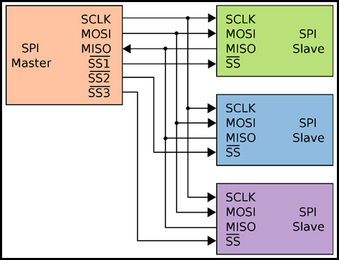
In addition to these three lines, if the microcontroller exchanges data with several peripheral devices, the forth line SS may be also used. Refer to figure 6-13 below.
SS - Slave Select - is additional pin used for specific device selection. It is active only in case the microcontroller is in slave mode, i.e. when the external - master device requires data exchange.
When operating in SPI mode, MSSP module uses in total of 4 registers:
SSPSR shift register not directly available
The first three registers are writable/readable and can be changed at any moment, while the forth register, since not available, is used for converting data into serial format.
As seen in figure 6-14, the central part of the SPI module consists of two registers connected to pins for receive, transmit and synchronization.
Shift register SSPRS is directly connected to the microcontroller pins and used for data transmission in serial format. The SSPRS register has its input and output and shifts the data in and out of device. In other words, each bit appearing on input receive line simultaneously shifts another bit toward output transmit line.
The SSPBUF register Buffer is a part of memory used to temporarily hold the data written to the SSPRS until the received data is ready. Upon receiving all 8 bits of data, that byte is moved to the SSPBUF register. This double buffering of the received data SSPBUF allows the next byte to start reception before reading the data that was just received. Any write to the SSPBUF register during transmission/reception of data will be ignored. Since having been the most accessed, this register is considered the most important from the programmers point of view.
Namely, if mode settings are neglected, data transfer via SPI actually means to write and read data from this register, while another acrobatics such as moving registers are automatically performed by hardware.
Prior to initializing the SPI, it is necessary to specify several options:
Master mode SCK pin is the clock output ;
Slave mode SCK pin is the clock input ;
Data input phase- middle or end of data output time SMP bit ;
Baud Rate only in Master mode ; and
Slave select mode Slave mode only.
Data to transmit should be written to the buffer register SSPBUF. Immediately after that, if the SPI module operates in master mode, the microcontroller will automatically perform the following steps 2, 3 and 4. If the SPI module operates as Slave, the microcontroller will not perform these steps until the SCK pin detects clock signal.
This data is now moved to the SSPSR register and the SSPBUF register is not cleared.
Synchronized with clock signal, this data is shifted to the output pin MSB bit first while the register is simultaneously being filled with bits through input pin. In Master mode, the microcontroller itself generates clock, while the Slave mode uses external clock pin SCK.
The SSPSR register is full once the 8 bits of data have been received. It is indicated by setting the BF and SSPIF bits. The received data that byte is automatically moved from the SSPSR register to the SSPBUF register. Since data transfer via serial communication is performed automatically, the rest of the program is normally executed while data transfer is in progress. In that case, the function of the SSPIF bit is to generate interrupt when one byte transmission is completed.
At last, the data stored in the SSPBUF register is ready for use and moved to any register available.
I C mode Inter IC Bus is especially suitable when the microcontroller and integrated circuit, which the microcontroller should exchange data with, are within the same device. It is commonly about another microcontrollers or specialized, cheap integrated circuits belonging to the new generation of so called smart peripheral components memories, temperature sensors, real-time clocks etc.
Similar to serial communication in SPI mode, data transfer in I C mode is synchronous and bidirectional. This time only two pins are used for data transfer. These are the SDA Serial Data and SCL Serial Clock pins. The user must configure these pins as inputs or outputs through the TRISC bits.
Perhaps it is not directly visible. By observing particular rules protocols, this mode enables up to 122 different components to be simultaneously connected in a simple way by using only two valuable I/O pins. Briefly, everything works as follows: Clock necessary to synchronize the operation of both devices is always generated by the master device microcontroller and its frequency directly affects baud rate. There are protocols allowing maximum 3,4 MHz clock frequency so called high-speed I C bus, but the clock frequency of the most frequently used protocol is limited to 100 KHz. There is no limit in case of minimal frequency.
When master and slave components are synchronized by the clock, every data exchange is always initialized by master. Once the MSSP module has been enabled, it waits for a Start condition to occur. First the master device sends the START bit logic zero through the SDA pin, then the 7-bit address of the selected slave device, and finally, the bit which requires data write 0 or read 1 to that device. Accordingly, following the start condition, the eight bits are shifted into the SSPSR register. All slave devices share the same transmission line and all will simultaneously receive the first byte, but only one of them has the address to match.
Fig. 6-20 Master and Slave Configuration
Once the first byte has been sent only 8-bit data are transmitted, master goes into receive mode and waits for acknowledgment from the receive device that address match has occurred. If the slave device sends acknowledge data bit 1, data transfer will be continued until the master device microcontroller sends the Stop bit.
This is the simplest explanation of how two components communicate. If needed, this microcontroller is able to control more complicated situations when 1024 different components, shared by several different master devices, are connected. Such devices are rarely used in practice and there is no need to discuss them at greater length.
Figure below shows the block diagram of the MSSP module in I C mode.
Fig. 6-22 MSSP Block Diagram in I C Mode
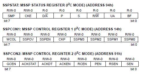
The MSSP module uses six registers for I C operation. Some of them are shown in figure above:
SPI master mode - This bit determines input data phase.
1 - Logic state is read at end of data output time; and
0 - Logic state is read in the middle of data output time.
SPI slave mode This bit must be cleared when SPI is used in Slave mode.
1 - Slew rate control disabled for standard speed mode 100kHz ; and
0 - Slew rate control enabled for high speed mode 400kHz.
CKE - Clock Edge Select bit selects synchronization mode.
1 - Data is transmitted on rising edge of clock pulse 0 - 1 ; and
0 - Data is transmitted on falling edge of clock pulse 1 - 0.
1 - Data is transmitted on falling edge of clock pulse 1 - 0 ; and
0 - Data is transmitted on rising edge of clock pulse 0 - 1.
D/A - Data/Address bit is used in I C mode only.
1 - Indicates that the last byte received or transmitted was data; and
0 - Indicates that the last byte received or transmitted was address.
P - Stop bit is used in I C mode only.
1 - STOP bit was detected last; and
0 - STOP bit was not detected last.
S - Start bit is used in I C mode only.
1 - START bit was detected last; and
0 - START bit was not detected last.
R/W - Read Write bit is used in I C mode only. This bit holds the R/W bit information following the last address match. This bit is only valid from the address match to the next Start bit, Stop bit or not ACK bit.
1 - Transmit is in progress; and
0 - Transmit is not in progress.
UA - Update Address bit is used in 10-bit I C mode only.
1 - Indicates that it is necessary to update the address in the SSPADD register; and
0 - Address in the SSPADD register is correct and does not need to be updated.
During data receive in SPI and I C modes
1 - Receive complete. The SSPBUF register is full; and
0 - Receive not complete. The SSPBUF register is empty.
During data transmit in I C mode only
1 - Data transmit in progress does not include the bits ACK and STOP ; and
0 - Data transmit complete does not include the bits ACK and STOP.
WCOL Write Collision Detect bit
1 - Collision detected. A write to the SSPBUF register was attempted while the I C conditions were not valid for a transmission to start; and
SSPOV Receive Overflow Indicator bit
1 - A new byte is received while the SSPSR register still holds the previous data. Since there is no space for new data receive, one of these two bytes must be cleared. In this case, data in SSPSR is lost; and
0 - Serial data is correctly received.
SSPEN - Synchronous Serial Port Enable bit determines the microcontroller pins function and initializes MSSP module:
1 - Enables MSSP module and configures pins SCK, SDO, SDI and SS as the source of the serial port pins; and
0 - Disables MSSP module and configures these pins as I/O port pins.
1 - Enables MSSP module and configures pins SDA and SCL as the source of the serial port pins; and
CKP - Clock Polarity Select bit is not used in I C master mode.
1 - Idle state for clock is a high level; and
0 - Idle state for clock is a low level.
0 - Holds clock low. Used to provide more time for data stabilization.
SSPM3-SSPM0 - Synchronous Serial Port Mode Select bits. SSP mode is determined by combining these bits:
SPI master mode, clock Fosc/16
SPI master mode, clock Fosc/64
SPI master mode, clock output TMR /2
SPI slave mode, SS pin control enabled
SPI slave mode, SS pin control disabled, SS can be used as I/O pin
I C slave mode, 7-bit address used
I C slave mode, 10-bit address used
I C master mode, clock Fosc / 4 SSPAD 1
I C slave mode, 7-bit address used,START and STOP bits enable interrupt
I C slave mode, 10-bit address used,START and STOP bits enable interrupt
Table 6-3 Synchronous Serial Port Mode Select Bits
GCEN - General Call Enable bit
1 - Enables interrupt when a general call address 0000h is received in the SSPSR; and
0 - General call address disabled.
ACKSTAT - Acknowledge Status bit
In I C Master Transmit mode only
1 - Acknowledge was not received from slave; and
0 - Acknowledge was received from slave.
In I C Master Receive mode only
ACKEN - Acknowledge condition Enable bit
1 - Initiate acknowledge condition on SDA and SCL pins and transmit ACKDT data bit. It is automatically cleared by hardware; and
0 - Acknowledge condition is not initiated.
1 - Enables data receive in I C mode; and
PEN - STOP condition Enable bit
1 - Initiates STOP condition on pins SDA and SCL. Afterwards, this bit is automatically cleared by hardware; and
0 - STOP condition is not initiated.
RSEN - Repeated START Condition Enabled bit
1 - Initiates START condition on pins SDA and SCL. Afterwards, this bit is automatically cleared by hardware; and
0 - Repeated START condition is not initiated.
SEN - START Condition Enabled/Stretch Enabled bit
1 - Initiate START condition on pins SDA and SCL. Afterwards, this bit is automatically cleared by hardware; and
0 - START condition is not initiated.
The most common case is when the microcontroller operates as a master and the peripheral component as a slave. This is why this book covers just this mode. It is also considered that the address consists of 7 bits and device contains only one microcontroller one master device.
In order to enable MSSP module in this mode, it is necessary to do the following:
Set baud rate SSPADD register, turn off slew rate control by setting the SMP bit of the SSPSTAT register and select master mode SSPCON register. After the preparation has been finished and module has been enabled SSPCON register: SSPEN bit, one should wait for internal electronics to signal that everything is ready for data transmission, i.e. the SSPIF bit of the PIR1 register is set.
This bit should be cleared by software and after that, the microcontroller is ready to start communication with peripherals.
Data Transmission in I C Master Mode
Each clock condition on the SDA pin starts with logic zero 0 which appears upon setting the SEN bit of the SSPCON2 register. Even enabled, the microcontroller has to wait a certain time before it starts communication. It is the so called Start condition during which internal preparations and checks are performed. If all conditions are met, the SSPIF bit of the PIR1 is set and data transfer starts as soon as the SSPBUF register is loaded.
Since maximum 112 integrated circuits may simultaneously share the same transmission line, the first data byte must contain address which matches only one slave device. Each component has its own address listed in the proper data sheet. The eighth bit of the first data byte specifies direction of data transmission, the microcontroller is to send or receive data. In this case, it is all about data receive and the eighth bit therefore is logic zero 0.
Fig. 6-28 Data Transmission in I C Master Mode
When address match occurs, the microcontroller has to wait for the acknowledge data bit. The slave device acknowledges address match by clearing the ASKSTAT bit of the SSPCON2 register. If the match properly occurred, all bytes representing data are transmitted in the same way.
Data transmission ends by setting the SEN bit of the SSPCON2 register. The so called STOP condition occurs, which enables the SDA pin to receive pulse condition: Start - Address - Acknowledge - Data - Acknowledge. Data - Acknowledge - Stop.
Fig.6-29 Data Transmission in I C Master Mode
Data Reception in I C Master Mode
Preparations for data reception are similar to those for data transmission, with exception that the last bit of the first sent byte containing address is logic one 1. It specifies that master expects to receive data from addressed slave device. With regard to the microcontroller, the following events occur:
After internal preparations are finished and START bit is set, slave device starts sending one byte at a time. These bytes are stored in the serial register SSPSR. Each data is, after receiving the last eighth bit, loaded to the SSPBUF register from where it can be read. By reading this register, the acknowledge bit is automatically sent, which means that master device is ready to receive new data.
At the end, similar to data transmission, data reception ends by setting the STOP bit:
Fig. 6-30 Data Reception in I C Master Mode
Start - Address - Acknowledge - Data - Acknowledge. Data - Acknowledge - Stop.
In this pulse condition, the acknowledge bit is sent to slave device.
In order to synchronize data transmission, all events taking place on the SDA pin must be synchronized with the clock generated in master device. This clock is generated by a simple oscillator whose frequency depends on the microcontroller s main oscillator frequency, value written to the SSPADD register and the current SPI mode.
The clock frequency of the mode described in this book depends on selected quartz crystal and the SPADD register. The formula used to calculate it is shown in figure below.
When the microcontroller communicates with peripheral components, it may happen that data transfer fails for some reason. In that case, it is recommended to check the status of some bits which can clarify the problem. In practice, the state of these bits is checked by executing a short subroutine after each byte transmission and reception just in case.
WCOL SPCON,7 - If you try to write a new data to the SSPBUF register while another data transmit/receive is in progress, the WCOL bit will be set and the contents of the SSPBUF register remains unchanged. Write does not occur. After this, the WCOL bit must be cleared in software.
BF SSPSTAT,0 - In transmit mode, this bit is set when the CPU writes to the SSPBUF register and remains set until the byte in serial format is shifted from the SSPSR register. In receive mode, this bit is set when data or address is loaded to the SSPBUF register. It is cleared when the SSPBUF register is read.
SSPOV SSPCON,6 - In receive mode, this bit is set when a new byte is received by the SSPSR register via serial communication, whereas the previously received data has not been read from the SSPBUF register yet.
SDA and SCL Pins - When SPP module is enabled, these pins turns into Open Drain outputs. It means that these pins must be connected to the resistors which, at the other end, are connected to positive power supply.
Fig. 6-32 Open Drain Output Resistors
In order to establish serial communication in I C mode, the following should be done:
Setting Module and Sending Address:
Value to determine baud rate should be written to the SSPADD register;
SlewRate control should be turned off by setting the SMP bit of the SSPSTAT register;
In order to select Master mode, binary value 1000 should be written to the SSPM3-SSPM0 bits of the SSPCON1 register;
The SEN bit of the SSPCON2 register should be set START condition ;
The SSPIF bit is automatically set at the end of START condition when the module is ready to operate. It should be cleared;
Slave address should be written to the SSPBUF register; and
When the byte is sent, the SSPIF bit interrupt is automatically set when the acknowledge bit has been received from the Slave device.
Data is to be send should be written to the SSPBUF register;
When the byte is sent, the SSPIF bit interrupt is automatically set upon the acknowledge bit has been received from Slave device; and
In order to inform the Slave device that transmit is complete, STOP condition should be initiated by setting the PEN bit of the SSPCON register.
In order to enable receive the RSEN bit of the SSPCON2 register should be set;
The SSPIF bit signals data receive. When data is read from the SSPBUF register, the ACKEN bit of the SSPCON2 register should be set in order to enable sending acknowledge bit; and
In order to inform Slave device that transmit is complete, the STOP condition should be initiated by setting the PEN bit of the SSPCON register.
1 Getting Started: SPI Date: SPISPI Overview and Use of the PICmicro Serial Peripheral Interface In this presentation, we will look at what the Serial.
2000 Microchip Technology Inc. Preliminary DS00735A-page 1 INTRODUCTION This application note describes the implementation of the PICmicro MSSP module for Master.
PIC16F887 features all the components which modern microcontrollers normally have. It is an ideal solution in applications such as the control of different processes.
Lab 2 EE4341 2. This lab For this lab you will need the following equipment: An evaluation board with a PIC18F4520 and a Microchip Serial Flash EEPROM.
Managed Security Service Provider, who provides security services for companies
Members of the Society of Specialist Paralegals
Microsoft Smooth Streaming Protocol, a computer networking protocol designed to support adaptive media streaming
Mobile Service Switching Point, see Service Switching Point
Medicare Shared Savings Program, established by section 3022 of the Affordable Care Act, which rewards healthcare organizations that improve the health of their overall patient population while limiting cost-growth; 1 rewarding organizations that produce healthier patients at lower costs.
Master Synchronous Serial Port, a module of a PIC microcontroller that is used for communication with other peripherals. 2
https://www.cms.gov/Medicare/Medicare-Fee-for-Service-Payment/sharedsavingsprogram/index.html
Retrieved from https://en.wikipedia.org/w/index.php.title MSSP oldid 698618806
Categories: Disambiguation pages.